

Designing HDI PCBs
In complex electronic devices such as mobile / cellular phones, touch-screen devices, laptop computers, digital cameras, and even military applications such as smart munitions, HDI PCBs are used to achieve high performance with excellent space utilization. However, with the increased density of components and traces in an HDI design comes the challenge of proper impedance-controlled routing. This is crucial to maintain signal integrity, EMI suppression, and power management in the board.
Inadequate component placement can severely impact the signal integrity of an pcb hdi. For instance, placing sensitive components closer to heat-generating areas or allowing insufficient clearance between them can cause crosstalk, impedance mismatches, and EMI susceptibility. Similarly, routing critical traces such as clock signals and data buses through hotspots can also affect signal integrity.
Achieving the proper impedance in high-speed signals is another significant challenge in an HDI PCB layout. It requires careful use of differential pairs, length matching, and effective design techniques to minimize interference. Also, maintaining an optimal aspect ratio for vias is crucial to avoid excessive capacitance and noise.
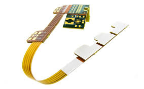
Challenges in Designing HDI PCBs
Moreover, the more dense a PCB becomes, the more susceptible it is to electromagnetic interference (EMI). Traces located close to each other can induce voltages in adjacent loops of wire, which can interfere with the operation of other electronics within the device. To reduce this issue, performing EMI modeling in the early stages of the design process is vital.
Finally, the thermal performance of an HDI PCB is a major concern. This is mainly because of the limited amount of space available. To ensure optimal performance, designers should consider factors such as using advanced dielectric materials with higher thermal conductivity to facilitate heat dissipation and prevent shorting. They should also avoid placing high-speed signals near power and ground planes to reduce the risk of EMI.
While many of the aforementioned challenges are critical to successful HDI PCB designs, they can be overcome with collaboration with fabricators, careful planning, and advanced tools. For example, the right CAD tool can make designing an HDI circuit board easy with features such as impedance calculating, automated microvia placement, and 3D visualization. Additionally, selecting a fabrication partner with experience and capability in handling HDI technology is essential to reduce manufacturing defects and other quality issues. Moreover, it is important to invest in ongoing training and professional development to stay up-to-date on emerging technologies. This will allow designers to effectively implement these technologies into their projects and create the best products for their customers.